- Industry news
Industry news
- Category news
Category news
- Reports
- Key trends
- Multimedia
- Journal
- Events
- Suppliers
- Home
- Industry news
Industry news
- Category news
Category news
- Reports
- Key trends
- Multimedia
- Events
- Suppliers
SEMICON Japan 2025 live: Boschman showcases silver sintering for semiconductor packaging
Key takeaways
- Boschman Advanced Packaging Technology is showcasing its patent silver sintering system at SEMICON Japan 2025, which enables the sintering of multiple dies with varying thicknesses.
- The technology is key for electric vehicle power electronics that require thermal resistance and reliability.
- Boschman emphasizes that the industry is shifting from silicon to wide-bandgap materials for improved performance.
At SEMICON Japan 2025 in Tokyo, Boschman Advanced Packaging Technology is presenting its patent technologies, including its silver sintering system, a die attach technology in semiconductor packaging.
Sintering is a thermal process of bonding loose, fine particles into a solid mass using heat or pressure without fully melting them. Boschman’s silver sintering is said to provide a “void-free and strong bond with high thermal and electrical conductivity.”
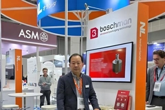
“Our high-precision dynamic insert pressure control technologies enable sintering multiple dies with different die thicknesses. With our patent individual insert, we can control the pressure,” Jae Young Kim, account director for East Asia at Boschman, tells Packaging Insights live from the show floor.
The company notes that power electronics are key in the conversion of electrical power, and power electronic modules need to contain multiple power semiconductors.
.webp) Boschman provides encapsulation and bonding processes for semiconductor packaging solutions.
Boschman provides encapsulation and bonding processes for semiconductor packaging solutions.
“Nowadays, sintering machines are needed for electric vehicle power packages,” Kim shares.
Integrated approach
Boschman points out that the conventional semiconductor material, silicon, is reaching its physical limits in terms of power density, switching frequency, operating temperature, and breakdown voltage. The industry is therefore looking into wide-bandgap materials to replace silicon, such as silicon carbide and gallium nitride.
These materials need new designs and processes to handle higher temperatures and provide better thermal resistance, performance, and reliability for back-end semiconductor packaging.
“We have two system platforms. The first one is a sintering machine, and the second one is a film assisted molding,” says Kim.
Boschman’s integrated approach, combining development support services with mass-production industrial equipment, aims to provide advanced packaging technologies that deliver improved high-temperature capability, thermal resistance, and reliability.
