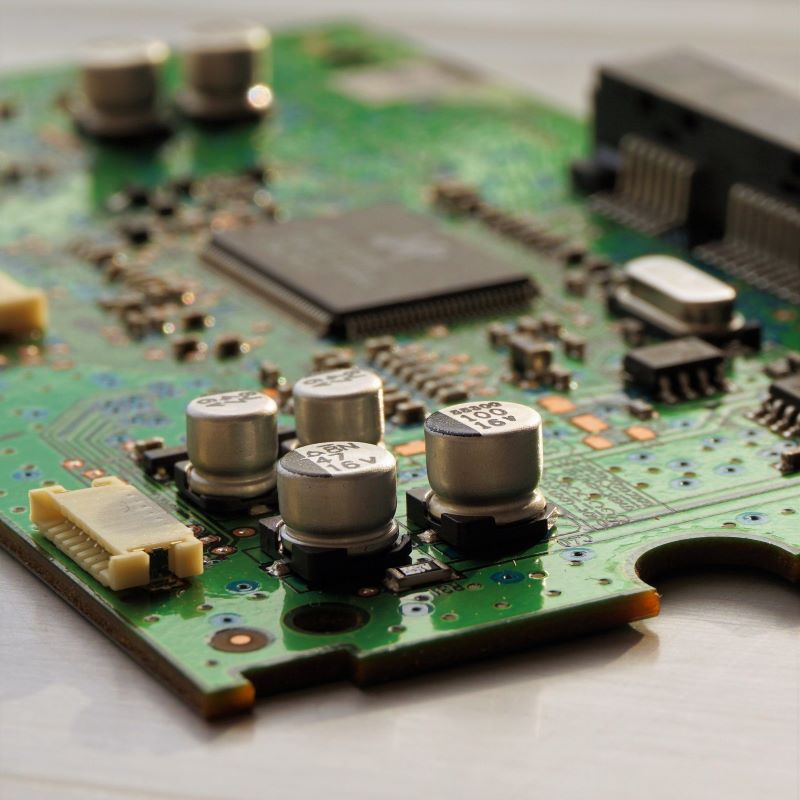
Samsung Electronics launches alliance for next-generation packaging tech


29 Jun 2023 --- To address the rapid growth in the chiplet market for mobile and high-performance computing (HPC) applications, Samsung Electronics is launching the Multi-Die Integration (MDI) Alliance in collaboration with its partner companies and “major players” in memory, substrate packaging and testing.
The advanced semiconductor technology provider announced its latest foundry technology innovations and business strategy at the 7th annual Samsung Foundry Forum (SFF) 2023 in San Jose, US and is addressing customer needs in the AI sphere through advanced semiconductor technology.
As part of its business strategy to solidify its competitiveness as a leading foundry service, Samsung Foundry expanded applications of its 2-nanometer process and specialty process. It also expanded production capacity at its Pyeongtaek fab Line 3.
Customized packaging
Samsung Electronics launched the MDI Alliance for next-generation packaging technology and continued progress in the foundry ecosystem with Samsung Advanced Foundry Ecosystem (SAFE) partners.
The MDI Alliance leads innovation in stacking technology by forming a packaging technology ecosystem for 2.5 D and 3 D Heterogeneous Integration. With partners across the ecosystem, Samsung will provide a one-stop turnkey service to better support customers’ technological innovation.
 Samsung Electronics addresses customers’ AI needs through advanced semiconductor technology.The tech giant plans to respond to customer and market needs by developing customized packaging solutions tailored to the individual needs of various applications, including HPC and automotive.
The company will also host the SFF 2023 in South Korea in July and expand to Europe and Asia later in the year to meet customers in each region.
New tech designs
Following the SFF, Samsung also hosted the Samsung Advanced Foundry Ecosystem (SAFE) Forum yesterday in San Jose, US, under the theme “Accelerating the Speed of Innovation.”
Together with partners across electronic design automation (EDA), design solution partners (DSP), outsourced semiconductor assembly and test (OSAT), cloud and IP, Samsung is promoting mutual growth of the foundry ecosystem to power the success of customers.
Samsung has long supported stronger collaboration between partners across the foundry ecosystem, advancing the boundaries of design infrastructure from 8-inch to the latest GAA process. Samsung and its 23 EDA partners now offer over 80 design tools and the company is also collaborating with 10 OSAT partners to develop 2.5 D and 3 D packaging design solutions.
Samsung provides product design services to various customers from start-ups to industry leaders through strong partnerships with nine DSP partners with extensive expertise in Samsung Foundry processes, and nine Cloud partners.
“Through extensive collaboration with our SAFE partners, Samsung Foundry is helping simplify designs that are becoming even more complex amid the application of the most advanced processes and new technologies such as heterogeneous integration,” explains Jong-wook Kye, executive vice president and head of Design Platform Development, Foundry Business at Samsung Electronics.
Edited by Natalie Schwertheim